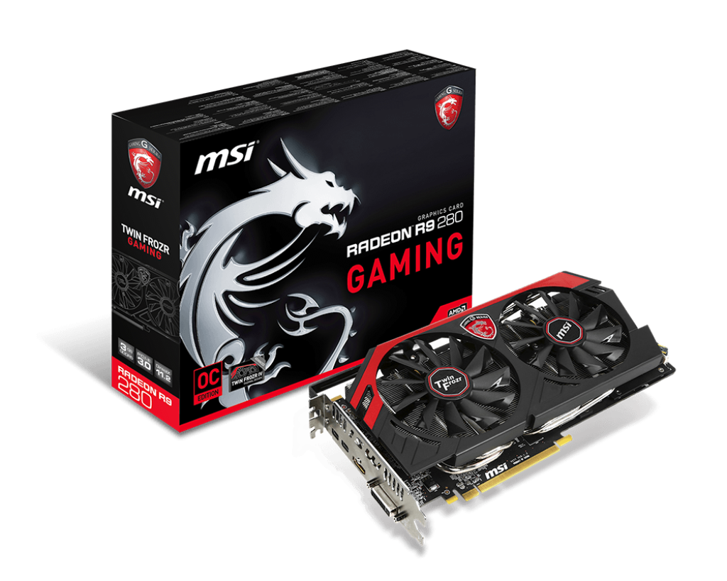
Radeon R9 280 GAMING 3G
AMD Radeon™ R9 280
PCI Express x16 3.0
933MHz Core (Boost Clock:1000MHz) (OC mode)
933MHz Core (Boost Clock:972MHz) (Gaming mode)
933MHz Core (Boost Clock:933MHz) (Silent mode)
933MHz Core (Boost Clock:972MHz) (Gaming mode)
933MHz Core (Boost Clock:933MHz) (Silent mode)
5000
3072
GDDR5
384 bits
Y
250
1x6-Pin, 1x8-Pin
500
269x128x37 mm
849
12 API
4.3
CrossFireX
Up to 6 displays with the use of a DP MST Hub
240
DL-DVI-I x1Max Resolution: 2560 x 1600 @60 Hz
1 (version 1.4a)
Max Resolution: 3840x2160 @30 Hz
4096x2160 @24 Hz
Max Resolution: 3840x2160 @30 Hz
4096x2160 @24 Hz
2(version 1.2)
Max Resolution: 4096x2160 @ 50 Hz
Max Resolution: 4096x2160 @ 50 Hz
400
© AMD, and the AMD Arrow logo, Radeon, FreeSync, and combinations thereof are trademarks of Advanced Micro Devices, Inc. DirectX and Microsoft are registered trademarks of Microsoft Corporation in the US and other jurisdictions. PCI Express is a registered trademark of PCI-SIG Corporation. Vulkan and the Vulkan logo are trademarks of the Khronos Group Inc. Other product names are for identification purposes only and may be trademarks of their respective companies.
All images and descriptions are for illustrative purposes only. Visual representation of the products may not be perfectly accurate. Product specification, functions and appearance may vary by models and differ from country to country. All specifications are subject to change without notice. Although we endeavor to present the most precise and comprehensive information at the time of publication, a small number of items may contain typography or photography errors. Some products and configuration may not be available in all markets or launch time differs. Supplies are limited. We recommend you to check with your local supplier for exact offers and detail specifications.
‘Boost Clock Frequency’ is the maximum frequency achievable on the GPU running a bursty workload. Boost clock achievability, frequency, and sustainability will vary based on several factors, including but not limited to: thermal conditions and variation in applications and workloads. ‘Game Frequency’ is the expected GPU clock when running typical gaming applications, set to typical TGP (Total Graphics Power). Actual individual game clock results may vary. © 2024 Micro-Star Int'l Co.Ltd. MSI is a registered trademark of Micro-Star Int'l Co.Ltd. All rights reserved.
